
Durable Electronics Applications
Electronics built for harsh environment and space-based platforms operate where conventional semiconductors reach their limits fastest.
The Challenge
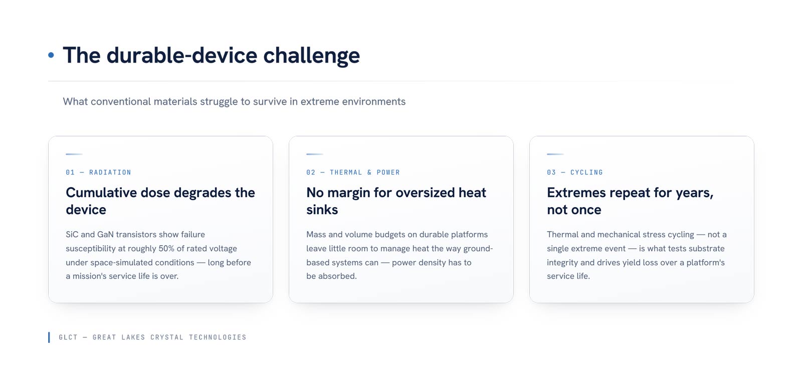
Even the wide-bandgap materials that dominate today’s high-reliability power and RF designs carry known vulnerabilities once they are in deployment.
In space and deep-earth-simulated conditions, current transistors have shown failure susceptibility, and current schottky diodes have exhibited catastrophic single-event burnout, with unacceptable leakage-current degradation. Add mass and thermal budgets that leave little room for oversized heat sinks or shielding, and the result is a persistent gap: platforms that need to survive years of radiation exposure, thermal cycling, and sustained power density without the margin conventional materials assume
The Solution
Optimizing The Extremes with Diamond
Single-crystal CVD diamond addresses this gap at the material level rather than through added shielding or derating. Its 5.5 eV bandgap and carrier mobility near 4,000 cm²/V·s at room temperature pair with breakdown voltage above 10 MV/cm, hole mobility above 3,800 cm²/V·s, and thermal conductivity above 22 W/cm·K — properties that hold up under the mechanical and thermal stability demands of vacuum operation. On radiation tolerance specifically, diamond is considered a nearly ideal material for radiation detection and is radiation-hard up to several megagrays of photon and electron exposure, and up to 10^15 neutrons or high-energy protons per cm² — an order of survivability that puts it in a different category from the WBG materials described above. Diamond also offers greater inherent radiation hardness from the outset than power SiC and GaN devices, which have well-documented radiation-effect problems.
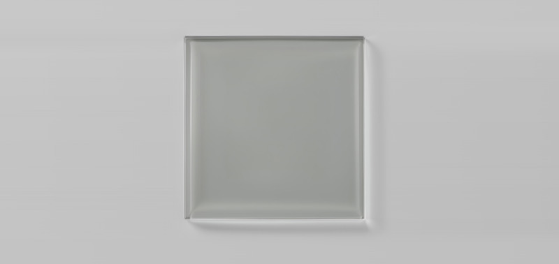
GLCT single-crystal diamond thermal products


Applications