
High-Power Electronics Applications
As power electronics push toward higher voltages, higher switching frequencies, and less room to dissipate heat, the semiconductor substrate itself has become the limiting variable.
The Challenge
High-power electronics have run into a materials ceiling
Current wide-bandgap devices pushed power electronics further than silicon ever could. But every generation of higher voltage, higher switching frequency, and higher current density asks the substrate underneath to do two things at once: survive the electric field, and move the heat out fast enough that the device doesn’t derate itself into failure. Silicon carbide and standard substrates are approaching the limit of doing both at once.
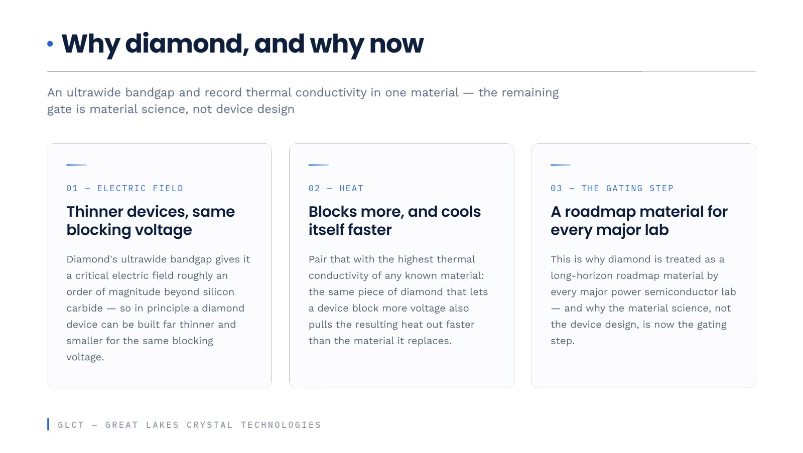
Diamond’s ultrawide bandgap gives it a critical electric field roughly an order of magnitude beyond silicon carbide — meaning a diamond device can, in principle, be built far thinner and smaller for the same blocking voltage. Pair that with the highest thermal conductivity of any known material, and the same piece of diamond that lets a device block more voltage also pulls the resulting heat out faster than the material it replaces. This is why diamond is treated as a long-horizon roadmap material by every major power semiconductor lab, and why the material science, not the device design, is now the gating step.
The Solution
Why Boron-Doped Diamond
Substitute a boron atom for a carbon atom in the diamond lattice and it introduces an accessible acceptor level — a hole in the lattice’s bonding structure that conducts current. This is p-type doping, and it is the only diamond doping chemistry that has reached device-grade maturity: boron-doped diamond has been used to demonstrate Schottky diodes, p-channel MOSFETs, and high-voltage device structures in published research.
The equivalent n-type chemistry — donor doping, typically with phosphorus — has no such head start. Phosphorus sits deeper in diamond’s band structure than boron does, which makes the resulting carriers harder to activate and the doping far less efficient. It’s an active, unsolved area of materials research, which is exactly where GLCT is directing its next development effort.
GLCT single-crystal diamond thermal products



Applications